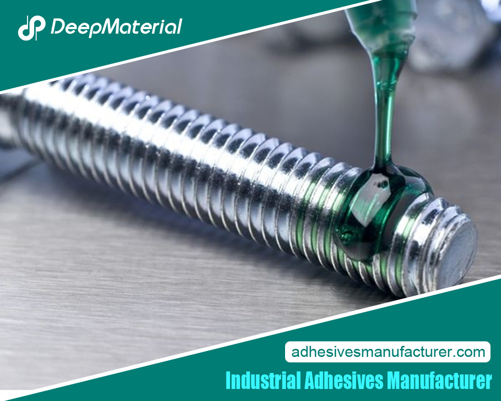
PCB Potting Compound

In the intricate world of electronics manufacturing, printed circuit boards (PCBs) serve as the foundation of modern technology. To enhance their durability and reliability, PCB potting compounds have emerged as a transformative solution. These compounds provide a protective enclosure for electronic components, shielding them from environmental factors, mechanical stresses, and contaminants. By encapsulating sensitive circuitry, PCB potting compounds ensure the longevity and performance of electronic devices, making them indispensable across industries. This comprehensive exploration delves into the realm of PCB potting compounds, uncovering their formulations, applications, benefits, and their pivotal role in safeguarding the heart of electronic systems.
Introducing PCB Potting Compounds
In the ever-evolving landscape of electronics, the quest for improved durability, reliability, and longevity has led to innovative solutions, among which PCB potting compounds stand out. PCB potting compounds, also known as encapsulation compounds, offer a robust protective layer that shields sensitive electronic components from harsh environmental conditions, mechanical stress, and potential contaminants. This advancement has revolutionized how we safeguard electronic devices, ensuring optimal performance even in challenging settings.
The primary purpose of PCB potting compounds is to encapsulate or “pot” electronic components within a solid, protective casing. This casing not only acts as a barrier against moisture, dust, chemicals, and vibrations but also enhances thermal conductivity. As electronic devices become smaller and more intricate, the risks associated with external factors damaging or interfering with their functionality increase. PCB potting compounds address these concerns by providing a seamless, conformal coating that maintains the components’ integrity and connections.
One of the key benefits of using PCB potting compounds is their versatility. We formulate these compounds to cater to various application requirements, from aerospace and automotive industries to consumer electronics and renewable energy systems. We can tailor them to achieve specific properties such as flexibility, high-temperature resistance, flame retardancy, and electrical insulation. Manufacturers can choose from various potting compounds to best suit their product’s demands, ensuring optimal performance under diverse conditions.
Moreover, PCB potting compounds offer a cost-effective solution for extending the lifecycle of electronic devices. By reducing the wear and tear caused by external factors, companies can minimize the need for frequent repairs and replacements, ultimately leading to enhanced customer satisfaction and reduced downtime. As industries continue to push the boundaries of technological innovation, PCB potting compounds emerge as a fundamental tool in preserving the functionality and reliability of cutting-edge electronics.
Challenges in Electronics Protection
In today’s rapidly evolving technological landscape, electronic devices have become integral to our daily lives, powering everything from communication to transportation. However, as the complexity and miniaturization of these devices increase, so do the challenges associated with protecting them from various external factors. Ensuring the durability and reliability of electronics in the face of these challenges requires innovative solutions and strategies.
Environmental Factors
Frequently, various environmental conditions expose electronics to a wide range of challenges that can negatively impact their performance and longevity. Some key challenges include:
- Moisture and Humidity:High moisture and humidity levels can lead to corrosion, short circuits, and degradation of components.
- Temperature Extremes: Fluctuations in temperature, from extreme cold to intense heat, can cause the expansion and contraction of materials, leading to mechanical stress and potential failure.
- Chemical Exposure:Corrosive chemicals often expose electronics to conditions that can deteriorate component materials and compromise their functionality.
Mechanical Stress
The shrinking size of electronic components makes them more susceptible to mechanical stress, which can result from factors like:
- Vibration and Shock:In applications like automotive and aerospace, electronics are exposed to constant vibration and sudden shocks, potentially causing dislodgment or damage.
- Flexing and Bending:Wearable devices and flexible electronics require protection against bending and flexing, which can weaken connections and lead to failure.
EMI/RFI Interference
Electromagnetic interference (EMI) and radio-frequency interference (RFI) can disrupt the proper functioning of electronic devices. Mitigating these challenges requires:
- Shielding:Effective shielding techniques are necessary to prevent external electromagnetic signals from interfering with sensitive electronic circuits.
Size and Design Constraints
The demand for smaller, sleeker devices presents challenges in designing effective protective measures:
- Limited Space:Shrinking device sizes leave little room for conventional protection methods, necessitating innovative solutions that maintain performance.
Heat Dissipation
As electronic components become more powerful, managing heat dissipation becomes crucial to prevent overheating and potential damage:
- Thermal Management:Ensuring proper heat dissipation is essential to maintain optimal performance and prevent thermal stress.
Cost and Manufacturability
Balancing the need for robust protection with cost-effectiveness and ease of manufacturing is a challenge faced by electronics manufacturers:
- Material Selection:Choosing suitable protective materials that offer the desired properties while remaining cost-effective can be complex.
- Application Process:Manufacturers must seamlessly integrate protective coatings or compounds into production processes without adding complexity or cost.
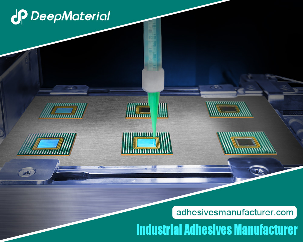
Mechanisms of Potting Compound Encapsulation
Potting compound encapsulation, a technique widely employed in electronics manufacturing, involves the application of protective compounds around sensitive components. This method offers a multifaceted defense against environmental factors, mechanical stress, and other challenges that electronic devices encounter. Understanding the mechanisms behind potting compound encapsulation sheds light on its effectiveness in enhancing electronic protection.
Barrier Protection
Potting compounds create a physical barrier that shields electronic components from various external elements, including:
- Moisture and Humidity:The impermeable nature of potting compounds prevents water from seeping into the electronic components, minimizing the risk of corrosion and short circuits.
- Dust and Contaminants:The solid casing formed by the potting compound blocks dust, dirt, and other contaminants from settling on or infiltrating the components.
Mechanical Shock Absorption
Electronics can experience mechanical shocks and vibrations that threaten their integrity. Potting compound encapsulation mitigates this through:
- Dampening:The compound absorbs and disperses mechanical shocks, reducing the impact on sensitive components and preventing dislodgment.
- Stress Distribution:The even distribution of mechanical stress across the encapsulated area minimizes the concentration of forces on individual components.
Thermal Management
Potting compounds play a vital role in managing heat generated by electronic components:
- Thermal Conductivity:Compounds with high thermal conductivity enhance heat dissipation, maintaining optimal operating temperatures and preventing overheating.
- Thermal Insulation:Some applications require potting compounds with insulating properties to prevent heat from affecting neighboring components.
Dielectric Properties
Electronics often require insulation to prevent electrical interference. Potting compounds offer:
- Dielectric Strength: Compounds with appropriate dielectric strength insulate components and prevent short circuits caused by electrical leakage.
Shock and Vibration Isolation
In applications subject to constant motion or vibration, potting compounds act as shock absorbers:
- Vibration Dampening:The compound’s flexibility and adhesive properties dampen vibrations, ensuring the longevity of components.
Customization and Application
We can tailor potting compounds to specific requirements:
- Flexibility:We can formulate compounds to accommodate flexible components without compromising their protection.
- Chemical Resistance:Tailored compounds resist chemical exposure, which is crucial in industrial and hazardous environments.
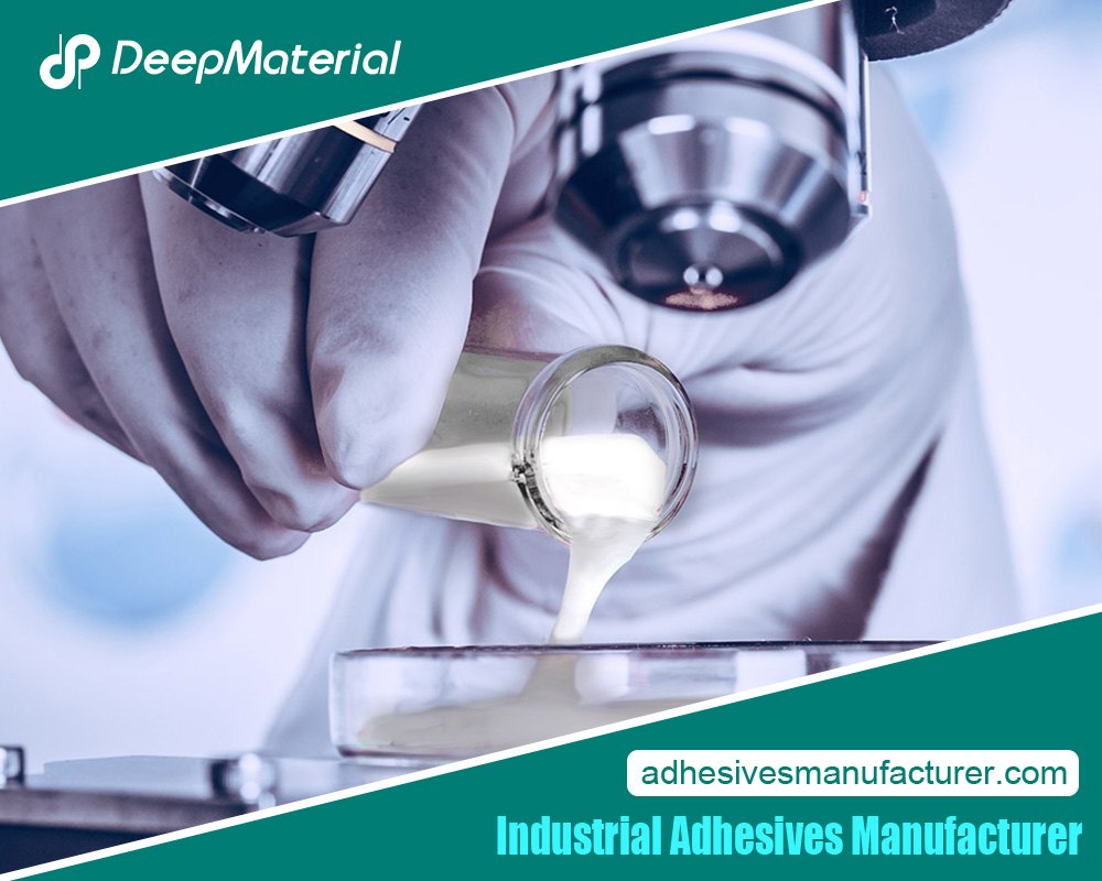
Materials for PCB Potting Compounds
PCB potting compounds safeguard printed circuit boards (PCBs) against environmental stressors and ensure their long-term reliability. These compounds encapsulate electronic components and create a protective barrier, shielding them from moisture, vibrations, thermal fluctuations, and mechanical impacts. The selection of appropriate materials for PCB potting compounds is vital to ensure optimal performance and durability. Several key considerations and material options come into play:
Thermal Conductivity and Dissipation
- Efficient heat dissipation is essential to prevent overheating of components.
- High thermal conductivity compounds enhance heat transfer away from sensitive parts.
- Materials like epoxy resins with added fillers, such as ceramic powders, can improve thermal properties.
Chemical Resistance
- Various chemicals, fuels, and solvents may expose PCBs.
- Potting compounds should resist degradation and maintain their properties.
- Polyurethane and silicone compounds are known for their chemical resistance.
Mechanical Protection
- PCBs can experience mechanical stresses from vibrations, shocks, and impacts.
- Potting materials with high mechanical strength and flexibility are preferred.
- Polyurethane compounds provide good mechanical protection while accommodating slight movements.
Environmental Sealing
- Potting materials must create an airtight seal to prevent moisture ingress.
- Compounds with low water absorption and excellent adhesion are vital.
- Silicone-based potting compounds offer reliable environmental sealing.
Dielectric Properties
- Potting compounds must maintain high dielectric strength to avoid electrical leakage.
- Electronic applications favor materials with low dielectric constants.
- Epoxy resins with suitable additives can provide desired dielectric properties.
Curing Time and Process
- The curing process affects production efficiency.
- Compounds with fast curing times can expedite manufacturing.
- Some potting materials require specific curing conditions like heat or UV light.
Long-Term Stability
- Potting compounds should withstand long-term exposure to harsh conditions.
- Factors such as UV radiation and temperature variations can impact stability.
- Silicone-based compounds often exhibit excellent long-term stability.
Regulatory Compliance
- PCB potting materials should adhere to industry regulations.
- Considerations include RoHS (Restriction of Hazardous Substances) compliance.
- Manufacturers often provide information on the regulatory status of their products.
Epoxy Resins for PCB Encapsulation
Epoxy resins have emerged as a critical component in electronics, particularly for Printed Circuit Board (PCB) encapsulation or potting. This process involves encasing electronic components and circuits within an epoxy resin to protect against environmental factors like moisture, dust, chemicals, and mechanical stress. Epoxy resins offer a range of benefits that make them an ideal choice for PCB encapsulation, ensuring the longevity and reliability of electronic devices.
Key features and advantages of using epoxy resins for PCB encapsulation include:
- Chemical Resistance:Epoxy resins exhibit remarkable resistance to various chemicals, including solvents, oils, and acids. This property ensures that the encapsulated PCBs remain functional and durable even when exposed to harsh environments.

- Electrical Insulation:Epoxy resins possess excellent electrical insulation properties. They help prevent short circuits and electrical leakage by providing a protective barrier around sensitive electronic components, thus enhancing the device’s overall reliability.
- Mechanical Protection:Epoxy encapsulation adds a layer of automatic protection to PCBs. It guards against physical impact, vibration, and shocks, making them suitable for applications in rugged environments.
- Thermal Stability:Epoxy resins maintain their stability over a wide temperature range. This property is essential for electronics operating in extreme cold and high-temperature conditions.
- Adhesion and Bonding:Epoxy resins adhere well to various materials used in electronic assemblies, such as PCB substrates, connectors, and components. This strong bond further enhances the structural integrity of the assembly.
- Customization:We can formulate epoxy resins to meet specific requirements, such as flexibility, transparency, or flame resistance. This versatility allows manufacturers to tailor the encapsulation material to their device’s needs.
- Protection Against Moisture and Environmental Factors:Epoxy-encapsulated PCBs are sealed against moisture and environmental contaminants, safeguarding them from corrosion and performance degradation.
- Enhanced Durability:By effectively shielding components from external elements, epoxy resin encapsulation extends the lifespan of electronic devices, reducing the need for maintenance or replacement.
Silicone Potting Compounds
Due to their remarkable properties and versatility, silicone potting compounds have emerged as a popular choice for encapsulating printed circuit boards (PCBs). These compounds offer exceptional protection against environmental factors, mechanical stresses, and thermal challenges. Here’s an exploration of the features and advantages of silicone potting compounds:
Superior Environmental Sealing
- Silicone compounds create a robust barrier against moisture, dust, and contaminants.
- Their excellent adhesion properties ensure a reliable seal around components.
- Silicone’s hydrophobic nature prevents water ingress and subsequent damage.
High Thermal Resistance
- Silicone potting compounds exhibit remarkable thermal stability.
- They can withstand a wide temperature range without losing their mechanical properties.
- This property makes them suitable for applications in both high and low-temperature environments.
Flexibility and Shock Absorption
- Silicone’s inherent flexibility accommodates mechanical movements and vibrations.
- It acts as a shock absorber, protecting delicate components from impacts and stresses.
- This property is beneficial in applications subject to frequent handling or external forces.
Excellent Dielectric Properties
- Silicone’s high dielectric strength prevents electrical leakage and interference.
- It is an ideal choice for applications demanding reliable insulation.
- Electronic devices and circuits commonly use silicone potting compounds.
Long-Term Stability
- Silicone compounds maintain their properties over extended periods.
- They resist UV radiation, maintaining their integrity in outdoor and exposed settings.
- This stability contributes to the longevity and reliability of encapsulated PCBs.
Ease of Processing
- Silicone potting compounds are often available in two-part formulations that are easy to mix and apply.
- They can be cured at room temperature or with mild heating, reducing processing complexity.
- Quick curing times can accelerate production processes.
Compatibility with Various Substrates
- Silicone compounds adhere well to various materials, including metals, plastics, and ceramics.
- This compatibility enhances their versatility and suitability for diverse applications.
Regulatory Compliance
- Many silicone potting compounds meet industry standards such as RoHS compliance.
- Their low toxicity and absence of hazardous substances make them environmentally friendly.
Polyurethane Encapsulation Solutions
Polyurethane encapsulation solutions have gained significant traction in electronics, particularly their utilization as PCB potting compounds. This process involves encasing electronic components and circuits within polyurethane resin to shield against environmental factors, ensuring their longevity and reliability in various applications. The unique properties of polyurethane make it a compelling choice for PCB encapsulation, offering a range of benefits that enhance the protection and performance of electronic devices.
Advantages
- Flexibility and Ductility:Polyurethane resins are known for their flexibility and elasticity, allowing them to absorb mechanical stresses and vibrations without compromising the integrity of the encapsulated components. This property is precious in applications where the device might undergo movement or external forces.
- Excellent Adhesion:Polyurethane compounds adhere exceptionally well to various surfaces, including different PCB substrates and components. This strong bond enhances the structural stability of the assembly.
- Chemical Resistance:Polyurethane resins resist various chemicals, including solvents, oils, and acids. This attribute shields the encapsulated electronics from potentially corrosive agents, contributing to the device’s overall durability.
- Thermal Conductivity:Some polyurethane encapsulation formulations exhibit good thermal conductivity. This property assists in dissipating heat generated by electronic components, preventing overheating and ensuring optimal device performance.
- Protection Against Moisture and Contaminants:Polyurethane-encapsulated PCBs are sealed against moisture and environmental contaminants, safeguarding them from moisture-related issues such as corrosion and short circuits.
- Customization:Manufacturers can tailor polyurethane encapsulation solutions to meet specific requirements. This versatility allows for creating of compounds with varying hardness, flexibility, and other desired characteristics.
- Electrical Insulation:Polyurethane resins possess good electrical insulation properties. This insulation helps prevent electrical leakage, short circuits, and other electrical malfunctions.
- UV Resistance:Some polyurethane formulations offer UV resistance, making them suitable for outdoor applications where exposure to sunlight might be a concern.
Thermal Conductive Potting Compounds
Thermal management is a critical consideration in the field of PCB potting compounds, especially as electronic components continue to become more powerful and compact. Thermal conductive potting mixes have emerged as a specialized solution to dissipate heat from sensitive components efficiently, enhancing overall performance and longevity. Here’s an exploration of the significance and advantages of thermal conductive potting compounds:
Enhanced Heat Dissipation
- We engineer thermal conductive potting compounds to facilitate efficient heat transfer.
- They contain fillers such as ceramic or metal particles that aid in conducting heat away from components.
- These compounds minimize the risk of overheating, which can lead to performance degradation or even failure.
Improved Thermal Stability
- We design these compounds to maintain thermal properties over a wide temperature range.
- They offer stability even in demanding environments with extreme heat or rapid temperature fluctuations.
Reduction of Hotspots
- Electronic devices can develop hotspots when heat distribution is uneven.
- Thermal conductive potting compounds help distribute heat uniformly, reducing the likelihood of hotspots that could damage components.
Compatibility with Sensitive Components
- Many advanced electronic components are sensitive to high temperatures.
- We formulate thermal conductive potting compounds to provide adequate heat dissipation without harming delicate parts.
Customizable Thermal Conductivity
- Different applications have varying heat dissipation requirements.
- Thermal conductive potting compounds offer a range of thermal conductivities, allowing customization to specific needs.
Electrical Insulation
- While facilitating heat transfer, these compounds also maintain excellent electrical insulation properties.
- This dual functionality is crucial to prevent electrical leakage and short circuits.
Durability and Longevity
- We engineer thermal conductive potting compounds for long-term performance.
- They resist degradation even when exposed to continuous thermal cycling and other stressors.
Application Flexibility
- These compounds find applications in various industries, including electronics, automotive, telecommunications, and renewable energy.
- They suit potting components like power modules, LED arrays, and high-performance processors.
Process Efficiency
- Many thermal conductive potting compounds can be easily mixed and dispensed.
- Their curing times are optimized to ensure efficient manufacturing processes.
Protection Against Moisture and Contaminants
PCB potting compounds play a vital role in safeguarding electronic components, mainly printed circuit boards (PCBs), from the damaging effects of moisture and contaminants. These compounds offer a comprehensive protective barrier that seals sensitive parts within a resilient enclosure, ensuring optimal performance, longevity, and reliability.
- Moisture Barrier:PCB potting compounds create a robust moisture barrier that shields internal components from humidity, water, and condensation. This aspect becomes crucial for applications exposed to outdoor or harsh environments, as it prevents issues such as short circuits, corrosion, and performance degradation caused by moisture ingress.

- Protection:Potting compounds provide resistance against a wide range of chemicals, including corrosive substances and solvents, thereby shielding PCBs from potential chemical damage in industrial or chemical-rich settings.
- Dust and Particle Prevention:Potting compounds encapsulate electronic components, preventing the infiltration of dust, dirt, and particles that could disrupt connections, compromise performance, or cause overheating.
- Vibration and Shock Absorption:The potting process ensures that components are securely immobilized, absorbing vibrations and shocks encountered during transportation, operation, or mechanical stress, thus reducing the risk of damage.
- Thermal Management:Many potting compounds possess excellent thermal conductivity properties, facilitating heat dissipation and ensuring that components maintain optimal operating temperatures.
- Electrical Insulation:Potting compounds offer effective electrical insulation, preventing short circuits and protecting sensitive components from electrical interference or cross-talk.
PCB potting compounds provide an all-encompassing protective shield against moisture, contaminants, and various environmental stresses that can compromise electronic components and PCB functionality. By preserving the integrity of electronics, these compounds contribute to enhanced performance, increased device lifespan, and reduced maintenance costs, making them a critical component of advanced electronics manufacturing.
Vibration and Shock Absorption
One must consider vibration and shock absorption when adequately protecting electronic components on printed circuit boards (PCBs). PCB potting compounds, specially formulated materials designed to encapsulate and safeguard sensitive parts, play a pivotal role. These compounds exhibit remarkable vibration and shock absorption characteristics, ensuring the durability and longevity of electronics in various applications. Key features include:
- Damping Capabilities:PCB potting compounds possess inherent damping properties that allow them to dissipate vibrational energy. This approach minimizes the transmission of mechanical shocks and vibrations to delicate components, effectively preventing potential damage or malfunction.
- Enhanced Reliability:Integrating vibration and shock absorption into potting compounds significantly improves the reliability of electronic devices in demanding environments, such as automotive, aerospace, and industrial settings.
- Reduced Stress on Components:By absorbing and dispersing mechanical stresses caused by external factors like impacts and vibrations, these compounds protect PCBs from structural damage, solder joint fatigue, and microcracks.
- Improved Performance:Repressing vibrations and shocks ensures consistent performance of electronic components, maintaining signal integrity and preventing data loss or corruption.
- Longevity and Cost-Efficiency:With increased protection against mechanical wear and tear, PCBs potted with these compounds tend to have a longer operational lifespan, reducing maintenance and replacement costs.
- Design Flexibility:PCB potting compounds offer versatility in design, allowing engineers to optimize the potting process to achieve specific vibration and shock absorption requirements.
- Compatibility:These compounds are compatible with various electronic components, from delicate microchips to larger connectors and features, making them suitable for multiple applications.
Integrating vibration and shock absorption properties within PCB potting compounds is a critical solution to safeguarding electronic components against the detrimental effects of mechanical stresses. With their damping capabilities, increased reliability, and cost-effective benefits, these compounds contribute significantly to the performance and longevity of electronics in challenging environments.
Chemical and Solvent Resistance
Chemical and solvent resistance in PCB potting compounds is paramount when protecting sensitive electronic components in demanding environments. These specially formulated materials provide a robust shield against a wide range of chemicals, solvents, and environmental factors, ensuring the integrity and longevity of the encapsulated components. Key features include:
- Chemical Barrier:PCB potting compounds create a barrier that prevents corrosive chemicals, oils, and other substances from coming into direct contact with delicate components, mitigating the risk of damage and degradation.
- Solvent Repellence:These compounds exhibit a high degree of repellence to solvents, preventing them from permeating and compromising the integrity of the encapsulated electronics.
- Environmental Resilience:The chemical and solvent resistance of potting compounds equips electronic devices to withstand exposure to harsh environments, including industrial processes, automotive fluids, and outdoor elements.
- Material Compatibility:Engineers design PCB potting compounds to be compatible with various materials, ensuring their safe use alongside different electronic components without causing adverse reactions.
- Enhanced Reliability:The protection offered by chemical and solvent resistance translates to improved reliability, reducing the risk of premature component failure or malfunction due to chemical exposure.
- Extended Lifespan:The ability of potting compounds to resist chemical corrosion and solvent penetration contributes to the vast operational lifespan of electronics, resulting in reduced maintenance and replacement costs.
- Custom Formulations:Manufacturers can tailor potting compounds to meet specific chemical resistance requirements, allowing customization based on the application’s unique challenges.
Incorporating chemical and solvent resistance properties within PCB potting compounds is a critical defense mechanism against the potential harm caused by corrosive substances. By establishing a robust barrier and safeguarding components against chemical exposure, these compounds enhance electronic devices’ reliability, durability, and overall performance, particularly in environments where chemical and solvent exposure is a concern.
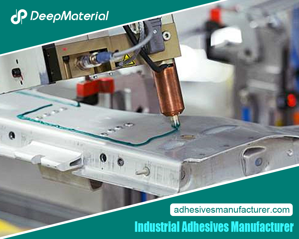
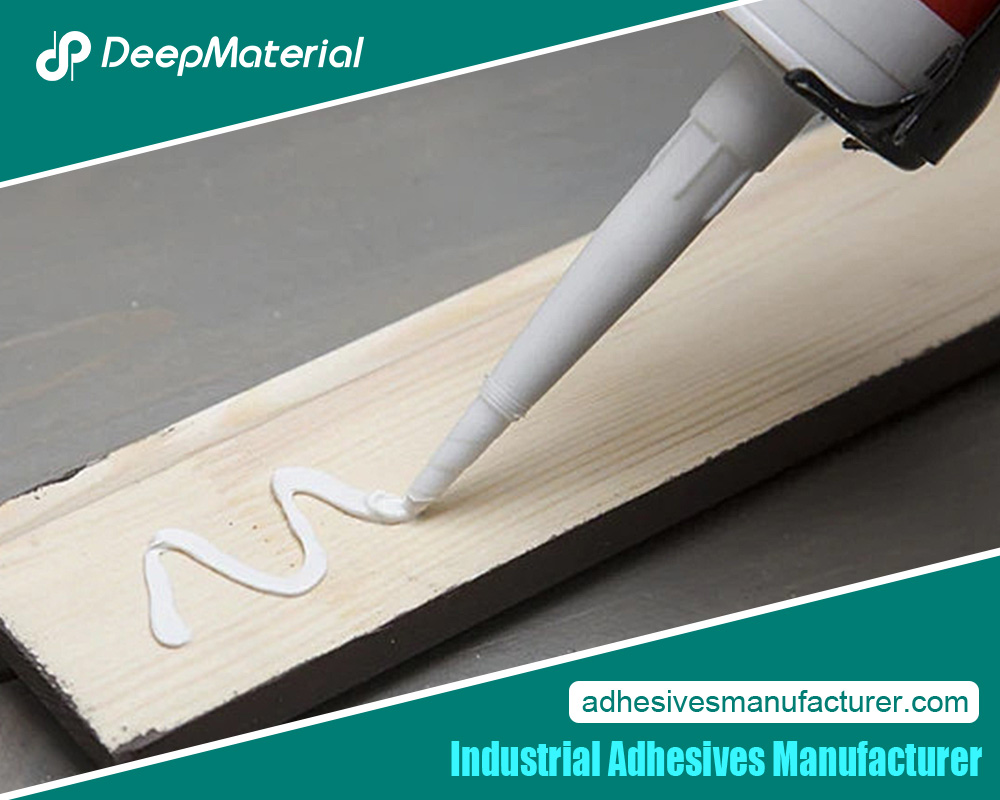
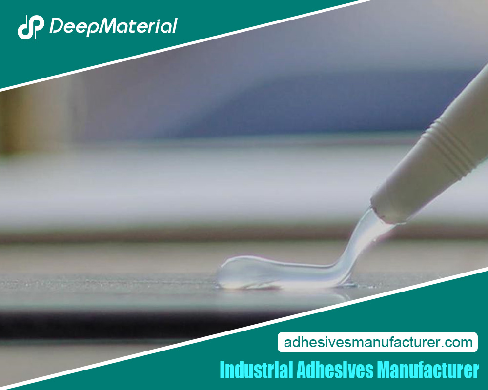
PCB Potting Techniques
PCB potting techniques encompass a range of methods employed to encapsulate and protect sensitive electronic components within a printed circuit board (PCB) assembly. These techniques play a crucial role in enhancing electronics’ durability, reliability, and longevity, particularly in challenging environments. Essential methods and considerations include:
- Encapsulation Materials:The choice of potting compound material is critical, with epoxy, silicone, polyurethane, and other formulations available to suit different application needs.
- Mold or Enclosure:Depending on the complexity of the assembly, manufacturers can opt for open molds or custom enclosures that accommodate the PCB and its components.
- Casting:This technique involves pouring the potting compound over the PCB to fully immerse the components, ensuring comprehensive protection against external factors.
- Vacuum Encapsulation:Using a vacuum to remove air bubbles and spaces within the potting compound enhances the uniformity and effectiveness of the encapsulation.
- Potting Gun Dispensing:Ideal for smaller-scale applications, potting guns enable precise and controlled dispensing of potting material directly onto components.
- Conformal Coating:While not traditional potting, a conformal coating selectively covers components, protecting them from moisture, dust, and chemicals.
- Thermal Management:Potting compounds with excellent thermal conductivity can also serve as a heat sink, dissipating excess heat generated by components.
- Adhesive Properties:Some potting compounds double as adhesives, securely affixing components to the PCB and preventing vibration-induced movement.
- Curing Time:Consideration of the potting material’s curing time is essential, affecting the production cycle and turnaround time.
- Testing:Quality control involves verifying that potting has been applied uniformly, without voids, and that components remain fully functional post-potting.
- Environmental Compatibility:Selecting a potting technique that aligns with the specific ecological conditions the PCB will encounter is vital for long-term reliability.
- Design Flexibility:PCB potting techniques should accommodate the assembly’s layout, component arrangement, and unique requirements.
PCB potting techniques offer a spectrum of approaches for encapsulating and safeguarding electronic components. By choosing the appropriate method and potting compound, manufacturers can ensure optimal protection, improved reliability, and extended lifespan of electronic devices, making them suitable for a wide range of applications and challenging environments.
Electronics in Harsh Environments
Deploying electronics in harsh environments introduces many challenges due to extreme conditions like temperature fluctuations, moisture exposure, chemical agents, and mechanical stresses. Printed Circuit Boards (PCBs) are at the heart of electronic devices, making them particularly vulnerable to these environmental factors. PCB potting compounds offer a strategic solution to fortify electronics against such challenges, ensuring durability, reliability, and sustained performance. This article delves into PCB potting compounds’ significance in safeguarding electronics in harsh environments.

Environmental Resilience
Electronics experience environmental stress in harsh conditions, such as extreme temperatures, humidity fluctuations, and corrosive agents. PCB potting compounds create a robust physical barrier that shields sensitive components from these adversities, enhancing the overall resilience of the electronic assembly.
Moisture and Chemical Protection
Moisture and chemicals pose significant threats to the functionality of electronic components. PCB potting compounds are engineered with moisture-resistant and chemically inert properties, preventing water ingress and chemical corrosion that can lead to short circuits and component failures.
Thermal Management
Harsh environments often entail temperature fluctuations that can impact electronics. Certain PCB potting compounds exhibit excellent thermal conductivity, serving as efficient heat sinks to dissipate excess heat generated by components, thereby maintaining optimal operating temperatures.
Vibration and Shock Absorption
Mechanical vibrations and shocks can compromise the structural integrity of electronics. PCB potting compounds with vibration and shock-absorbing properties help dampen these external forces, safeguarding delicate components from physical damage and ensuring sustained functionality.
Design Flexibility
PCB potting compounds offer design flexibility by conforming to PCB assemblies’ intricate shapes and layouts. This adaptability allows engineers to optimize the potting process for various form factors, ensuring complete coverage and protection of components.
Testing and Validation
Ensuring the effectiveness of PCB potting compounds involves rigorous testing and validation. Environmental tests, such as thermal cycling, vibration testing, and accelerated aging, validate the compound’s ability to withstand the intended harsh conditions and maintain long-term performance.
Industry Applications
PCB potting compounds find applications in diverse industries, including automotive, aerospace, marine, and industrial sectors. Their ability to mitigate environmental risks makes them invaluable for critical systems and devices deployed in these demanding environments.
Automotive Electronics Encapsulation
As automotive technology evolves, electronics integration within vehicles becomes increasingly sophisticated, driving safety, efficiency, and connectivity innovation. However, the automotive environment is inherently challenging, exposing electronics to extreme temperature variations, vibrations, moisture, and chemicals. For ensuring optimal performance and longevity, automotive electronics require robust protection. PCB potting compounds emerge as a crucial solution, providing a reliable shield against these adversities. This article explores how PCB potting compounds enhance the reliability of automotive electronics through effective encapsulation.
Demanding Environmental Conditions
Automotive electronics face various environmental challenges, including temperature fluctuations from cold to scorching heat, exposure to road salts, moisture ingress, and mechanical vibrations. These conditions can significantly impact the performance and lifespan of electronic components.
Moisture and Corrosion Protection
Moisture and corrosive agents present in the automotive environment pose a serious threat to electronic components. PCB potting compounds, formulated to resist moisture and chemicals, create a protective barrier that shields against water ingress and chemical corrosion, preserving the integrity of electronics.
Temperature Resilience
Extreme temperatures can cause thermal stress and affect the reliability of automotive electronics. Certain PCB potting compounds exhibit excellent thermal conductivity, dissipating heat generated by components and ensuring consistent operation across a wide temperature range.
Vibration and Shock Absorption
Automobiles experience constant vibrations and shocks due to road conditions and vehicle movement. PCB potting compounds with vibration and shock-absorbing properties minimize the transmission of these mechanical stresses to delicate electronics, reducing the risk of physical damage and failure.
Enhanced Reliability and Longevity
By providing a protective layer around electronic components, PCB potting compounds significantly enhance automotive electronics’ overall reliability and lifespan. Safety is paramount for critical systems like airbags, brakes, and engines.
Customized Solutions
Different automotive applications have varying encapsulation requirements. PCB potting compounds offer customization options, allowing engineers to select the most suitable material and technique based on the specific needs of each component and system.
Regulatory Compliance and Testing
Automotive electronics must adhere to stringent industry standards and regulations. PCB potting compounds that meet these standards undergo rigorous testing, ensuring their ability to withstand the unique challenges the automotive environment poses.
Aerospace and Defense Applications
Ensuring the utmost reliability is paramount in the aerospace and defense sectors, where mission-critical electronics operate in some of the most extreme and unforgiving environments. PCB potting compounds emerge as a vital component in achieving this goal, offering advanced encapsulation solutions that safeguard electronics against many challenges. Key considerations and benefits include:
- Extreme Temperature Extremes:Aerospace and defense electronics often encounter rapid temperature fluctuations, from the frigid cold of high altitudes to the scorching heat of engine compartments. PCB potting compounds with exceptional thermal conductivity provide adequate heat dissipation, maintaining consistent operation across these extremes.
- Vibration and Shock Resistance:Aircraft and military vehicles endure intense vibrations and shocks during operation. Potting compounds designed with vibration and shock-absorbing properties shield electronics from mechanical stresses, preventing damage and ensuring reliability in high-impact scenarios.
- Hermetic Sealing:The vacuum of space and the harsh conditions of military operations demand robust sealing against moisture, gases, and other contaminants. PCB potting compounds offer hermetic sealing that prevents ingress and preserves electronic components’ integrity.
- Chemical and Radiation Protection:Cosmic radiation and potentially corrosive chemicals expose aerospace electronics. Potting compounds with chemical resistance and radiation shielding properties defend against these hazards, preventing deterioration and malfunction.
- Mission-Critical Reliability: The reliability of aerospace and defense electronics is non-negotiable. PCB potting compounds contribute to the longevity and consistency of electronic components, ensuring they perform flawlessly in critical missions and operations.
- Customization for Specific Requirements:Different aerospace and defense applications have unique demands. You can tailor PCB potting compounds to meet specific requirements, ensuring compatibility with the particular challenges posed by each mission or operation.
- Industry Compliance:The aerospace and defense sectors adhere to rigorous standards and regulations. Potting compounds that meet these standards undergo extensive testing to guarantee their effectiveness in withstanding the demanding conditions of these applications.
PCB potting compounds play a pivotal role in aerospace and defense applications by fortifying electronics against temperature extremes, vibrations, shocks, moisture, chemicals, and radiation. By elevating the reliability, durability, and performance of electronics in these critical sectors, potting compounds contribute to the success of missions and operations, enhancing the safety and effectiveness of aerospace and defense systems.
Industrial Electronics Protection
Industrial electronics are pivotal in modern manufacturing processes, powering critical machinery and automation systems. Protecting these electronics from harsh environmental conditions, moisture, and mechanical stress is paramount to ensure their optimal performance and longevity. PCB potting compounds are crucial in this context. These compounds offer a robust solution to safeguard delicate electronics by creating a protective barrier that encapsulates components and circuitry. This article delves into the significance of industrial electronics protection through PCB potting compounds, highlighting their key benefits and applications.

Benefits of PCB Potting Compounds:
- Environmental Shielding:PCB potting compounds provide exceptional protection against moisture, dust, chemicals, and other contaminants compromising electronics’ reliability and functionality.
- Vibration and Shock Absorption:Industrial settings often involve heavy machinery and equipment, subjecting electronics to vibrations and shocks. Potting compounds act as shock absorbers, reducing the risk of mechanical stress-related failures.
- Thermal Management:Potting compounds with high thermal conductivity assist in dissipating heat generated by electronic components, maintaining optimal operating temperatures, and preventing overheating.
- Dielectric Properties:These compounds exhibit excellent dielectric properties, preventing electrical short circuits and enhancing insulation, which is crucial for electronics functioning safely.
- Corrosion Resistance:Potting compounds act as a protective barrier in corrosive environments, shielding electronics from rust and deterioration caused by exposure to harsh chemicals or moisture.
Applications of Industrial Electronics Protection:
- Automation Systems:Companies widely use potting compounds to protect PLCs, sensors, and control systems in automated manufacturing lines, ensuring uninterrupted operations and reduced downtime.
- Motor Drives and Inverters:Electronics controlling motors and inverters are prone to vibration-induced damage. Potting compounds extend their lifespan by mitigating mechanical stress.
- LED Lighting:Potting compounds safeguard sensitive LED drivers against temperature fluctuations, moisture, and external impacts, ensuring consistent and reliable illumination.
- Power Supplies:Potting compounds enhance the resilience of power supply units by shielding them from environmental factors and preventing electrical short circuits.
- Communication Equipment:From radio transmitters to data communication devices, potting compounds provide durability and protection for electronics responsible for seamless information exchange.
Advancements in Potting Compound Technology
Potting compound technology has undergone remarkable advancements, revolutionizing how electronics are protected and ensuring enhanced performance and longevity. These developments have significantly impacted the efficacy of PCB potting compounds, contributing to their effectiveness in safeguarding sensitive electronics. This section explores the cutting-edge advancements in potting compound technology and their pivotal role in PCB potting compounds.
Advancements in Potting Compound Technology
- Nano-Filled Formulations:Incorporating nanoparticles like silica or alumina enhances mechanical and thermal properties, elevating the compound’s overall performance and durability.
- Conductive Potting Compounds:For applications requiring electromagnetic interference (EMI) shielding, conductive potting compounds offer a dual advantage of protection and EMI mitigation.
- Low-Cure and Fast-Cure Compounds:Developing compounds with rapid curing times reduces production cycle times and enhances manufacturing efficiency.
- Flexible and Impact-Resistant Compounds:Advancements in the formulation have led to compounds that combine flexibility and impact resistance, ideal for electronics subjected to mechanical stress.
- Thermally Conductive Compounds:Highly efficient thermal management is achieved with compounds with excellent thermal conductivity, effectively dissipating heat.
- Optically Clear Compounds:Optically clear potting compounds allow for visual verification while providing protection in applications where visual inspection is essential.
- Biodegradable and Eco-Friendly Compounds:The industry’s focus on sustainability has led to the development of biodegradable and environmentally friendly potting compounds.
- Self-Healing Compounds:Some compounds can heal minor cracks, enhancing the longevity of the protection layer and ensuring prolonged electronics functionality.
Impact on PCB Potting Compounds
These advancements have revolutionized the domain of PCB potting compounds, elevating their capabilities to an unprecedented level:
- Higher Performance:Advanced formulations contribute to increased sensitive electronics’ durability, protection, and longevity.
- Diverse Applications:With conductive, flexible, thermally conductive, and optically clear options, potting compounds now cater to a broader range of applications.
- Efficiency and Productivity:Low-cure and fast-cure compounds expedite production processes, reducing time-to-market and boosting manufacturing efficiency.
- Reliability:Self-healing and impact-resistant compounds enhance the reliability of potting solutions, reducing maintenance and replacement needs.
The dynamic advancements in potting compound technology have ushered in a new era of innovation and reliability in PCB potting compounds. From enhanced mechanical properties to eco-friendly options, these developments have redefined the landscape of electronics protection, ensuring optimal performance, durability, and sustainability in various industrial applications.
Sustainability and Environmental Considerations
Sustainability and environmental considerations have emerged as crucial factors shaping modern technological advancements, including potting compound technology. As industries increasingly prioritize eco-friendly solutions, these considerations play a pivotal role in developing and applying potting compounds. Key aspects of sustainability and environmental consciousness in potting compound technology include:
- Biodegradable Formulations:Manufacturers invest in creating potting compounds that break down naturally over time, reducing their environmental impact.
- Low VOC Emissions:Volatile organic compound (VOC) emissions are minimized in newer formulations, contributing to better air quality and reduced greenhouse gas emissions.
- Recyclable Materials:Recyclable materials in potting compound production support the circular economy and reduce waste.
- Renewable Resources:Some potting compounds are derived from renewable resources, reducing reliance on fossil fuels and minimizing the carbon footprint.
- Energy-Efficient Manufacturing:Sustainable manufacturing processes, such as energy-efficient production and reduced water consumption, are being adopted to minimize resource consumption.
- Longevity and Durability:Potting compounds that enhance the durability and lifespan of electronics contribute to reduced electronic waste, as fewer replacements are needed.
- End-of-Life Considerations:Manufacturers are considering the disposal phase of potting compounds, developing solutions with minimal adverse effects when products end their lifecycle.
- Lifecycle Analysis:Conducting lifecycle assessments helps identify potential environmental impacts throughout a product’s lifecycle, enabling informed decisions.
Incorporating these sustainability principles into potting compound technology addresses environmental concerns and benefits businesses by aligning with consumer demands for environmentally friendly products and demonstrating corporate social responsibility. Integrating sustainability and ecological considerations into potting compound technology as industries evolve sets a positive trajectory for a greener and more sustainable future.
Future Trends in PCB Potting Compounds
The field of PCB potting compounds is on the cusp of transformational changes driven by rapid technological advancements and evolving industry needs. As electronics become more intricate and diverse, the future of PCB potting compounds is poised to introduce innovative solutions that address complex challenges and provide enhanced protection. In this section, we explore the anticipated trends in PCB potting compounds, offering a glimpse into the exciting developments shaping the industry.
Anticipated Future Trends:
- Nanotechnology Integration:Researchers expect to integrate nanoengineered materials and nanoparticles into potting compounds, enhancing mechanical, thermal, and electrical properties.
- Innovative Potting Compounds:Advancements in materials science will enable potting compounds with smart features, such as self-monitoring, self-repair, and adaptive responses to environmental changes.
- Biocompatible Formulations:The medical and wearable electronics sectors will see the rise of biocompatible potting compounds suitable for implantable devices and skin-contact applications.
- Enhanced Thermal Management:As electronics become more power-dense, potting compounds will focus on more efficient heat dissipation to prevent overheating.
- High-Frequency Applications:Potting compounds with improved dielectric properties will cater to high-frequency applications like 5G and advanced wireless communication systems.
- Environmentally Conscious Solutions:Sustainability will remain at the forefront, driving the development of biodegradable, recyclable, and low-VOC-emitting potting compounds.
- Customization and 3D Printing:Advances in 3D printing technologies will allow for customized potting solutions, enabling intricate designs and tailored protection.
- Conductive and EMI Shielding Compounds: As electronic devices become more interconnected, there will be a growing demand for conductive and EMI shielding potting compounds.
- Optical Transparency:Potting compounds will evolve to provide optical transparency, benefiting applications that require visual inspection or light transmission.
Impact on the Industry
These future trends in PCB potting compounds hold significant implications for industries:
- Innovative Applications:Incorporating nanotechnology, smart features, and tailored properties will expand the potential applications of potting compounds.
- Efficiency and Performance:Enhanced thermal management and high-frequency capabilities will ensure electronics’ efficiency and reliability.
- Sustainability Integration:Environmental considerations will shape compound formulations, aligning with industries’ eco-conscious objectives.
- Customization and Rapid Prototyping:3D printing and customization options will accelerate product development and reduce time-to-market.
- Interconnectivity and Communication:Integrating conductive and EMI shielding compounds will contribute to seamless interconnectivity in IoT and 5G.
PCB potting compounds stand as guardians of modern electronics, shielding vital components from the diverse array of challenges posed by external influences. Their role in preserving functionality, reliability, and longevity is paramount. As technology advances and industries demand devices that can withstand harsh conditions, PCB potting compounds will remain instrumental in driving innovation and efficiency. With ongoing research and improvements, these compounds are poised to shape the future of electronics protection, enabling the creation of smarter, more resilient devices that power our interconnected world.